- 您现在的位置:买卖IC网 > Sheet目录311 > AT24C04AN-10SI-2.7 (Atmel)IC EEPROM 4KBIT 400KHZ 8SOIC
Absolute Maximum Ratings*
Operating Temperature ........................................ ? 40 ° C to +85 ° C
Storage Temperature .........................................? 65 ° C to +150 ° C
Voltage on Any Pin
with Respect to Ground ........................................ ? 1.0V to +7.0V
Maximum Operating Voltage .......................................... 6.25V
*NOTICE:
Stresses beyond those listed under “Absolute
Maximum Ratings” may cause permanent dam-
age to the device. This is a stress rating only and
functional operation of the device at these or any
other conditions beyond those indicated in the
operational sections of this specification is not
implied. Exposure to absolute maximum rating
conditions for extended periods may affect device
reliability.
DC Output Current........................................................ 5.0 mA
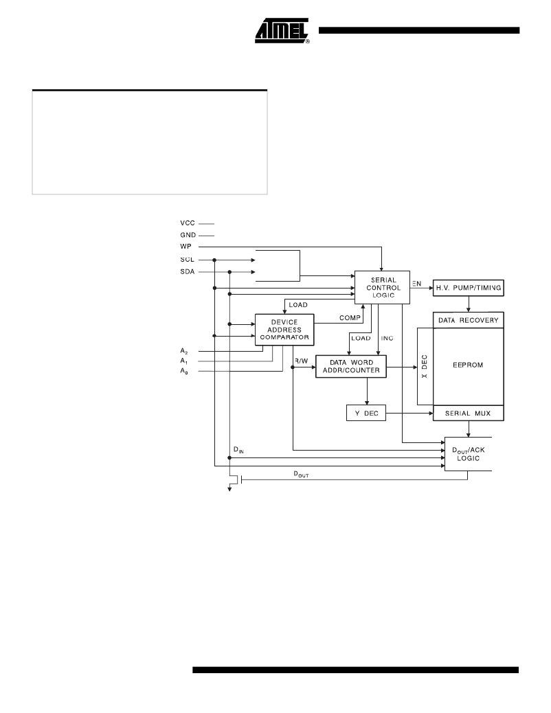
Figure 1. Block Diagram
S TART
S TOP
LOGIC
Pin Description
SERIAL CLOCK (SCL): The SCL input is used to positive edge clock data into each
EEPROM device and negative edge clock data out of each device.
SERIAL DATA (SDA): The SDA pin is bidirectional for serial data transfer. This pin is
open-drain driven and may be wire-ORed with any number of other open-drain or open
collector devices.
DEVICE/PAGE ADDRESSES (A2, A1, A0): The A2, A1 and A0 pins are device
address inputs that must be hardwired for the AT24C02A. As many as eight 2K devices
may be addressed on a single bus system. (Device addressing is discussed in detail
under Device Addressing, page 8).
2
AT24C02A/04A
0976Q–SEEPR–8/05
发布紧急采购,3分钟左右您将得到回复。
相关PDF资料
AT24C08B-PU
IC EEPROM 8KBIT 1MHZ 8DIP
AT24C1024B-TH25-B
IC EEPROM 1MBIT 1MHZ 8TSSOP
AT24C1024Y4-10YU-2.7
IC EEPROM 1MBIT 1MHZ 8SAP
AT24C11Y1-10YU-1.8
IC EEPROM 1KBIT 1MHZ 8MAP
AT24C128BY6-YH-T
IC EEPROM 128KBIT 1MHZ 8DFN
AT24C128C-XHM-B
IC EEPROM 128KBIT 400KHZ 8TSSOP
AT24C128Y1-10YU-1.8
IC EEPROM 128KBIT 400KHZ 8MAP
AT24C164-10SU-1.8
IC EEPROM 16KBIT 1MHZ 8SOIC
相关代理商/技术参数
AT24C04AN-10SI-2.7 SL383
功能描述:IC EEPROM 4KBIT 400KHZ 8SOIC RoHS:否 类别:集成电路 (IC) >> 存储器 系列:- 标准包装:96 系列:- 格式 - 存储器:闪存 存储器类型:FLASH 存储容量:16M(2M x 8,1M x 16) 速度:70ns 接口:并联 电源电压:2.65 V ~ 3.6 V 工作温度:-40°C ~ 85°C 封装/外壳:48-TFSOP(0.724",18.40mm 宽) 供应商设备封装:48-TSOP 包装:托盘
AT24C04AN-10SI-2.7-T
功能描述:IC EEPROM 4KBIT 400KHZ 8SOIC 制造商:microchip technology 系列:- 包装:带卷(TR) 零件状态:停產 存储器类型:非易失 存储器格式:EEPROM 技术:EEPROM 存储容量:4Kb (512 x 8) 时钟频率:400kHz 写周期时间 - 字,页:5ms 访问时间:900ns 存储器接口:I2C 电压 - 电源:2.7 V ~ 5.5 V 工作温度:-40°C ~ 85°C(TA) 安装类型:表面贴装 封装/外壳:8-SOIC(0.154",3.90mm 宽) 供应商器件封装:8-SOIC 基本零件编号:AT24C04 标准包装:3,000
AT24C04AN-10SQ-2.7
制造商:Atmel Corporation 功能描述:
AT24C04AN-10SU-1.8
功能描述:电可擦除可编程只读存储器 4K 2-WIRE 1M CYCLES - 10MS 1.8V RoHS:否 制造商:Atmel 存储容量:2 Kbit 组织:256 B x 8 数据保留:100 yr 最大时钟频率:1000 KHz 最大工作电流:6 uA 工作电源电压:1.7 V to 5.5 V 最大工作温度:+ 85 C 安装风格:SMD/SMT 封装 / 箱体:SOIC-8
AT24C04AN-10SU-2.7
功能描述:电可擦除可编程只读存储器 4K 2-WIRE 1M CYCLES - 10MS 2.7V RoHS:否 制造商:Atmel 存储容量:2 Kbit 组织:256 B x 8 数据保留:100 yr 最大时钟频率:1000 KHz 最大工作电流:6 uA 工作电源电压:1.7 V to 5.5 V 最大工作温度:+ 85 C 安装风格:SMD/SMT 封装 / 箱体:SOIC-8
AT24C04AN-10SU-2.7 SL383
制造商:Atmel Corporation 功能描述:EEPROM Serial-2Wire 4K-bit 512 x 8 3.3V/5V 8-Pin SOIC T/R
AT24C04AY1-10YI-1.8
制造商:未知厂家 制造商全称:未知厂家 功能描述:EEPROM
AT24C04AY1-10YI-2.7
制造商:未知厂家 制造商全称:未知厂家 功能描述:EEPROM
